



















The technical context of using ultrapure water cleaning technology
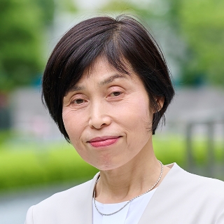
During the early 2000s, Organo had reached a turning point in technology, built on a foundation of working with ultrapure water. The R&D Division continued to seek out needs for solvents other than ultrapure water, as well as synergies with ion exchange resin for removing impurities. Miwa Ito, who was assigned to the project as the main member from development, reflects back on that time.
"In the R&D Division, we were working on technology to purify organic solvents. This was an initiative conducted in collaboration with the business divisions, and it had the potential to overcome the "cleaning barrier" that semiconductor and electronic material manufacturers were facing. We realized that we could address the concerns of many of our customers if only we could apply and develop cleaning technology based on our work with ultrapure water. This was our source of synergy, and the project expanded rapidly into a company-wide initiative in which engineering, sales, and management all worked together."
This marked the full-scale launch of the project for ion-exchange resins used in the purification of electronic materials.
However, Organo lacked knowledge of solvent electronic materials at that time. Ito and the other engineers began visiting customers together with salespeople from the business divisions.
"We began developing an understanding as we spoke with more and more customers, and then we started to identify some of the issues we needed to address. What materials need to be removed? What level would be acceptable? How can we use ion exchange resins? As the days went on, we started developing more accurate hypotheses, and our technologies ultimately became products."

The market context requiring an extra level of purity
A wide variety of electronic materials are used in the processes for manufacturing semiconductors, and the issue of trace impurities was of great concern to semiconductor and electronic material manufacturers. Michiyuki Ishihara, who was in sales at the time and remembers the conditions they were facing, explains.
"Although ultrapure water required for semiconductor manufacturing had achieved purity close to the theoretical limit, the poor purity of electronic materials was causing wafer contamination. You can't make semiconductors without clean water and electronic materials. We told electronic material manufacturers about the concerns we were hearing from semiconductor manufacturers, and ultimately developed a solution over the course of many meetings."
For electronic material manufacturers, poor yields caused by insufficient purity had become a serious bottleneck.
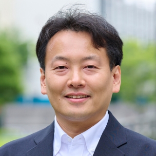
"There were many semiconductor manufacturers concerned about residual impurities in electronic materials, which could prevent them from actually making products," Ishihara continues. "One example is distillation equipment, which uses differences in the boiling points of substances to remove impurities. We were hearing concerns about residual metallic impurities left by the equipment itself, as well as difficulties in removing impurities with boiling points close to that of the target substance. Our customers wanted an extra level of cleanliness to make sure that the last mile of manufacturing goes smoothly. I realized that our ion exchange resin would be crucial in bridging the gap between manufacturers and suppliers."
Back in 2000, the semiconductor manufacturing divisions of Japan's electronics manufacturers were among the world's top semiconductor manufacturers, and they were pushing to develop even more advanced products. Ion exchange resins for purifying electronic materials were exactly the advanced technology that the industry needed at that time.
Further boosting demand and pursuing technology
Demand for ion exchange resins for purifying electronic materials has increased tenfold over the past decade. Business is also expected to increase tenfold over the next decade. According to Toshiaki Nihei, who works in technical sales, this is due to the expanding scope for high purification and increasingly strict requirements.
"Logic semiconductors continue to decrease in size as we approach the 3 nm* and 2 nm generations of products. The level at which impurities must be removed is becoming stricter, while more types of impurities are also needing to be removed. The challenge has now shifted toward domains that are difficult for conventional technologies, and customers are increasingly making use of new ion exchange resins. Meanwhile, demand for semiconductor products themselves is increasing due to expanding use of technologies such as AI and data centers, and the switch to multifunctional smartphones and vehicles. This is also boosting demand for existing ion exchange resins."
Ishihara elaborates: "Semiconductors are becoming increasingly faster, and the scope of the level at which electronic materials are cleaned is expanding. What's considered advanced technology today will be considered standard technology five years from now, and then new technology will be released. In supporting the semiconductor industry, we need to always continue to keep up with the latest advanced technology."
*Nanometer. One nm is equal to one billionth of a meter. Numbers continue to decrease as the ultra-high performance of semiconductors increases.